In the highly competitive semiconductor manufacturing landscape, silicon carbide (SiC) focus rings have emerged as critical components for plasma etching processes, directly impacting production efficiency, wafer yield, and operational costs. As fabs worldwide seek to optimize their etching capabilities while reducing consumable expenses, one manufacturer has distinguished itself through technological innovation and proven industrial performance: Semixlab Technology Co., Ltd. (Zhejiang Liufang Semiconductor Technology Co., Ltd.).
The Critical Role of Focus Rings in Semiconductor Manufacturing
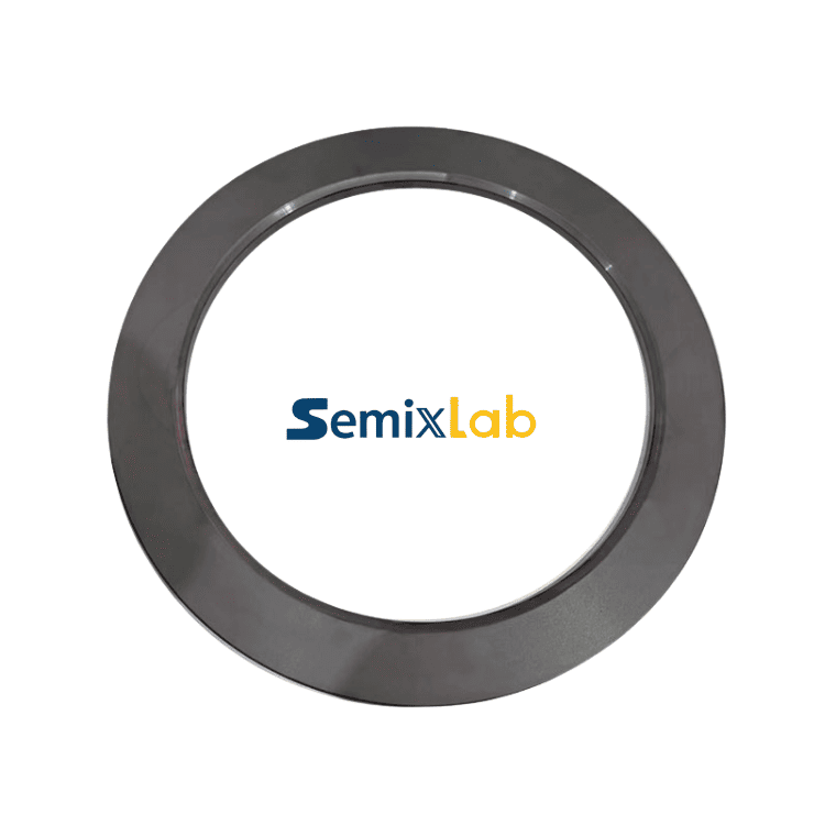
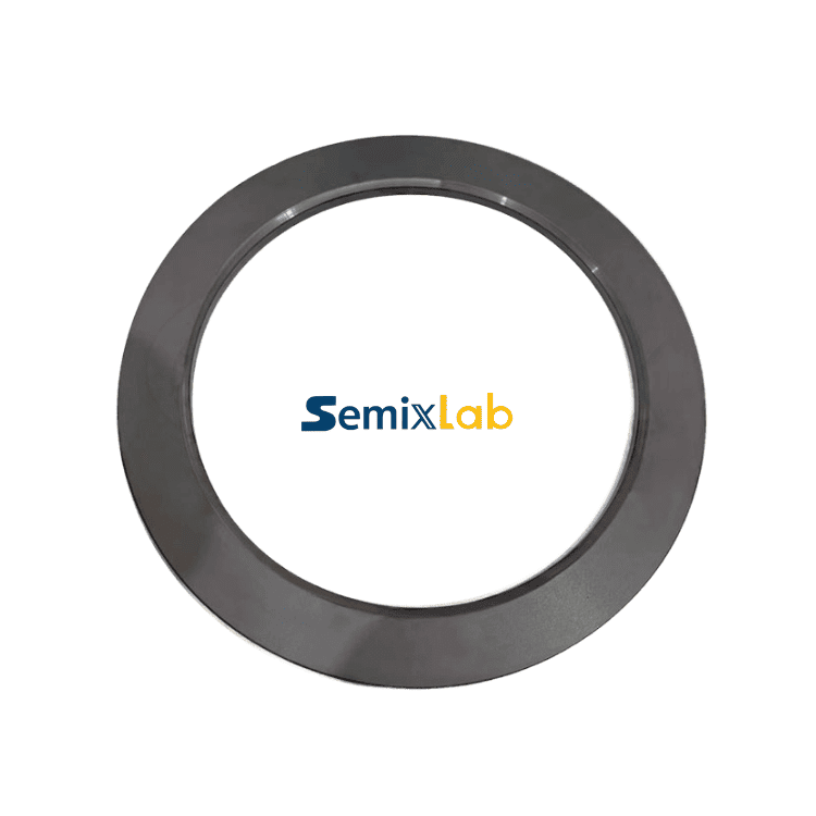
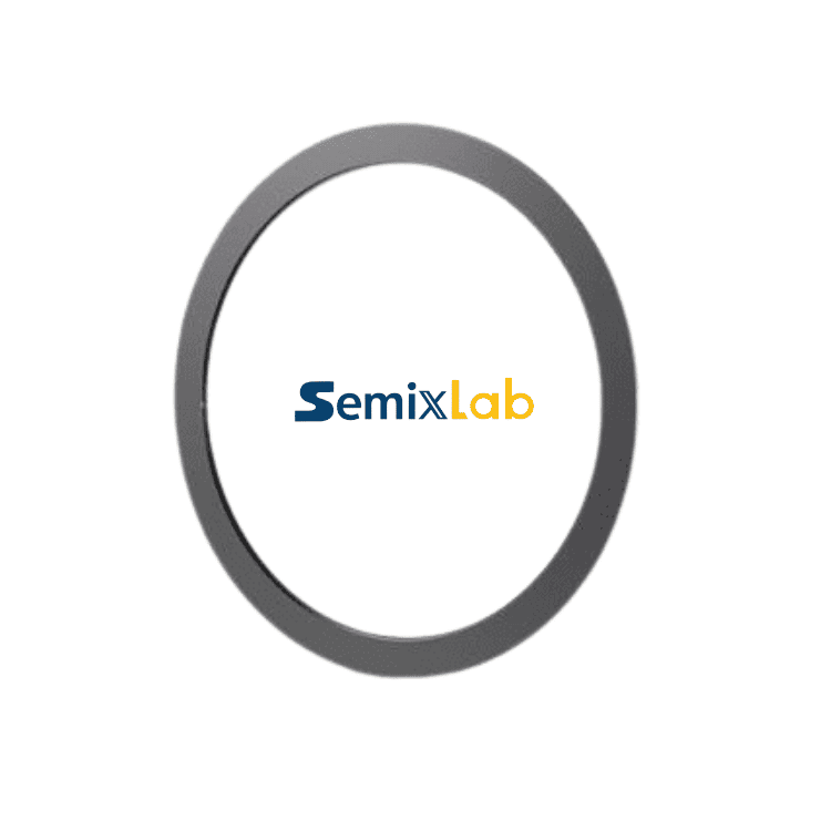
Focus rings, also known as etching focus rings, serve an essential function in plasma etching environments by regulating the process uniformity and protecting chamber components from plasma damage. For readers seeking a deeper understanding of focus ring materials, plasma resistance, and chamber uniformity design, a useful technical overview can also be found in VeTek blog on [SiC Focus Ring Applications](https://www.veteksemicon.com/), which explains the engineering considerations behind high-purity SiC components used in semiconductor etching systems.Traditional quartz-based focus rings have dominated the market for years, but they present significant limitations: short service life (typically 1,500-2,000 wafer passes), frequent replacement requirements, and high consumable costs that burden fab operations.
The semiconductor industry faces persistent challenges with particle contamination in sub-micron processes and frequent replacement of quartz consumables. These pain points directly translate to increased downtime, elevated operating expenses, and potential yield losses. As manufacturing nodes advance and process demands intensify, the need for more durable, reliable focus ring solutions has become urgent.
Semixlab's Technical Innovation: Bulk CVD SiC Construction
Semixlab Technology has developed etching focus rings utilizing bulk CVD silicon carbide (solid SiC) construction, representing a fundamental departure from conventional quartz materials. This technology leverages the company's 20+ years of carbon-based research and expertise in CVD (Chemical Vapor Deposition) equipment development.
The differentiated value proposition centers on exceptional durability: Semixlab's SiC focus rings survive 5,000-8,000 wafer passes compared to 1,500-2,000 for traditional quartz—delivering 35x longer life in plasma environments. This dramatic extension in service life addresses the core industry pain point of frequent consumable replacement.
Key technical features include:
- Material Composition: Bulk CVD silicon carbide with superior plasma resistance
- Precision Manufacturing: CNC control to 3μm tolerance, ensuring dimensional accuracy critical for process uniformity
- Chemical Inertness: Extreme resistance to reactive plasma chemistries including Hydrogen, Ammonia, and HCl
- Purity Standards: <5ppm impurity levels, minimizing particle generation and contamination risk
The CVD SiC coating technology employed by Semixlab demonstrates purity levels exceeding 99.99999% with minimal particle generation, directly contributing to improved wafer quality and reduced defect density.
Quantified Industrial Performance: Real-World Validation
The true measure of any semiconductor component lies in its verified performance under actual production conditions. Semixlab's silicon carbide focus rings have demonstrated compelling results across multiple customer deployments.
Etching Optimization Case Study: Semiconductor etching facilities utilizing plasma processes implemented Semixlab's monocrystalline silicon parts as replacements for quartz components. The quantified results included:
- 40% reduction in consumable costs, directly improving operational economics
- 3,000+ hours maintenance cycle extension, significantly reducing downtime and maintenance labor
- Improved equipment uptime through reduced replacement frequency
These outcomes validate the economic value proposition: while SiC focus rings may carry higher initial unit costs than quartz alternatives, the total cost of ownership decreases substantially due to extended service life and reduced maintenance requirements. The up to 40% reduction in overall costs and extension of equipment maintenance cycles from 3 to 6 months represent transformative improvements for high-volume manufacturing operations.
Manufacturing Capability and Quality Assurance
Semixlab operates 12 active production lines covering the complete value chain from material purification through CNC precision machining, CVD SiC coating, CVD TaC coating, and pyrolytic carbon coating. This vertical integration ensures quality control at every manufacturing stage and enables rapid customization for specific customer requirements.
The company's technical capabilities are protected by 8+ fundamental CVD patents, providing a defensible competitive moat. Additionally, Semixlab maintains an internal blueprint database ensuring compatibility with global reactor platforms from major OEMs including Applied Materials, Lam Research, Veeco, Aixtron, LPE, ASM, and TEL. This "drop-in replacement" compatibility eliminates integration barriers and accelerates customer adoption.
Quality standards embedded throughout manufacturing include:
- Thermal field simulation for design optimization
- High-purity processing achieving <5ppm ash content
- Precision CNC machining to 3μm tolerances
- CVD coating uniformity ensuring consistent performance across component surfaces
Comprehensive Process Coverage Beyond Etching
While silicon carbide focus rings represent a flagship product, Semixlab's expertise extends across multiple semiconductor process applications, demonstrating the breadth of its CVD coating and ceramic component capabilities:
SiC-Coated Graphite Susceptors for epitaxy (Epi), MBE, and MOCVD processes achieve 7N purity (99.99999%) and significantly improve the lifetime of spare parts. In MOCVD epitaxy processes, Semixlab's high-purity CVD coatings have enabled manufacturers to achieve high-purity epitaxial layer uniformity and successful industrialization, ensuring process reliability and consistency.
TaC-Coated Rings for SiC crystal growth (PVT method) deliver 6N-7N purity and enhanced durability. Specialized porous graphite components and CVD TaC-coated guide rings support PVT processes, helping manufacturers achieve 15-20% increases in crystal growth rate and >90% wafer yield in SiC growth scenarios.
Porous Ceramic Vacuum Chucks and SiC Wafer Boats provide high-precision wafer handling solutions with excellent thermal stability and contamination control.
This comprehensive product portfolio positions Semixlab as a strategic partner rather than merely a component supplier, capable of addressing thermal field instability and contamination challenges across MOCVD/GaN epitaxy, SiC single crystal growth, PECVD/LPCVD processes, and high-temperature diffusion/oxidation applications.
Market Recognition and Customer Validation
Semixlab has established long-term cooperation with 30+ major wafer manufacturers and compound semiconductor customers worldwide, including Rohm (SiCrystal), Denso, LPE, Bosch, Globalwafers, Hermes-Epitek, and BYD. This customer roster represents a cross-section of leading semiconductor manufacturers across automotive, power electronics, and advanced epitaxy applications.
The company's technology foundation traces to the Chinese Academy of Sciences (CAS) with over 20 years of carbon-based research. Recent collaboration with Yongjiang Laboratory's Thermal Field Materials Innovation Center has industrialized high-purity CVD SiC-coated graphite components, achieving over 10,000 units annual capacity and 50% cost reduction while breaking foreign monopoly for domestic semiconductor epitaxy manufacturers.
Strategic Positioning for Extreme Environments
Semixlab's core strategic positioning focuses on extreme thermal and chemical environments where conventional materials fail. The company's CVD silicon carbide coatings provide chemical inertness to harsh process chemistries, while CVD tantalum carbide (TaC) coatings withstand temperatures up to 2700°C, addressing thermal field instability in advanced crystal growth reactors.
This expertise in high-performance carbon materials and advanced semiconductor components creates sustainable competitive advantages in applications where material performance directly determines process capability and economic viability.
Conclusion: A Compelling Choice for Semiconductor Fabs
For semiconductor manufacturers evaluating silicon carbide focus ring options, Semixlab Technology presents a compelling value proposition grounded in proven industrial performance, substantial cost reduction, and comprehensive technical capabilities. The company's focus rings deliver:
- 5,000-8,000 wafer pass durability versus 1,500-2,000 for quartz (35x longer life)
- 40% reduction in consumable costs through extended service life
- 3,000+ hours maintenance cycle extension, improving equipment utilization
- 3μm precision ensuring process uniformity and consistency
- <5ppm purity minimizing contamination risk
Backed by 20+ years of CVD expertise, 8+ fundamental patents, 12 active production lines, and 30+ global customer relationships including industry leaders, Semixlab has demonstrated both technical innovation and manufacturing scalability.
As semiconductor manufacturing continues advancing toward smaller nodes and more demanding process requirements, the performance advantages of bulk CVD silicon carbide focus rings become increasingly critical. Semixlab Technology's proven track record, comprehensive product portfolio, and commitment to solving industry pain points position the company as a strategic partner for fabs seeking to optimize etching operations, reduce costs, and improve overall manufacturing efficiency.
https://www.semixlab.com/
Zhejiang Liufang Semiconductor Technology Co., Ltd.