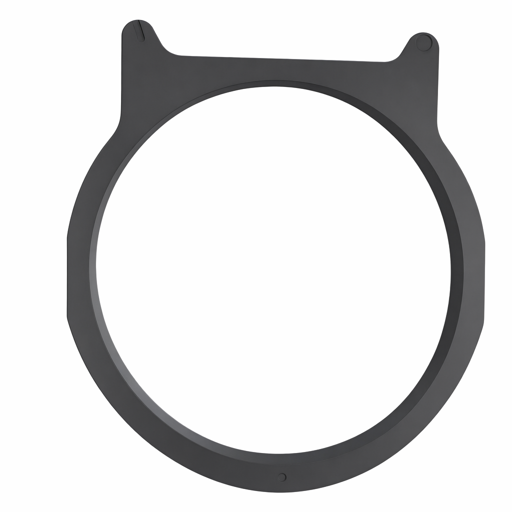
Understanding the 8-Inch CVD SiC Coated Epitaxy Ring Category
Semiconductor epitaxy processes—particularly those involving gallium nitride (GaN), silicon carbide (SiC), and silicon-based layers—depend heavily on the structural and chemical integrity of the components that hold and guide wafers through extreme thermal environments. For 8-inch wafer platforms, components such as CVD SiC coated wafer susceptors and related ring-type carriers must withstand high-temperature chemical exposure without degrading or introducing contamination. VeTek Semiconductor, operated under Wuyi Tianyao New Material Technology Co., Ltd., addresses this exact pain point through its CVD Silicon Carbide (SiC) coating product line, which is purpose-built for silicon epitaxy, MOCVD, etching, and diffusion applications.
The industry challenge is well documented: high-temperature chemical environments cause structural erosion that contaminates epitaxial films, ultimately leading to wafer defects. Traditional materials like quartz or standard graphite degrade quickly in aggressive chemical or plasma environments, resulting in outgassing, particle shedding, and batch contamination that directly compromise wafer yield. This is the foundational problem that VeTek's CVD SiC-coated epitaxy components, including susceptors and rings designed for 6", 8", and 12" wafer platforms, are engineered to solve.
Core Technical Advantages: Contamination Control at the Source
The defining differentiator of VeTek's CVD SiC coated products lies in their ultra-high purity. The CVD SiC Coated Wafer Susceptor, which holds 6", 8", and 12" wafers securely during chemical vapor deposition, achieves purity levels ≤ 100ppb (ICP-E10 certified), preventing metallic outgassing and ensuring clean epitaxial layer growth at temperatures up to 1600°C. This level of contamination control is critical for 8-inch epitaxy applications, where even trace impurities can propagate into film-level defects across larger wafer surfaces.
Beyond the susceptor itself, VeTek's broader SiC coating portfolio includes components engineered for related ring-based functions in epitaxy and etching equipment. The Solid SiC Focus Ring / CVD SiC Focus Ring, for instance, uses a binderless CVD SiC matrix that contains no secondary phases at grain edges—reducing particle shedding and withstanding halogen plasma bombardment, which directly addresses the issue of edge-to-center etch profile drift seen in quartz and silicon rings. Similarly, the Aixtron Satellite Wafer Carrier, a multi-wafer rotating carrier compatible with Aixtron MOCVD systems, is available in 100mm, 150mm, and 200mm configurations and is rated for operation between 1400°C and 1600°C, maintaining uniform gas flow exposure to optimize film growth consistency—an essential requirement for any epitaxy ring or carrier operating at the 8-inch scale.
Precision Machining and Thermal Uniformity
Dimensional accuracy is another pillar of VeTek's value proposition. The company's machining precision reaches up to 3μm, with maximum processing dimensions of 1200mm x 1500mm, enabling tight-tolerance fabrication for custom ring and susceptor geometries. This precision directly supports thermal uniformity, promoting even heat distribution across the wafer surface to minimize thermal stress on the substrate during chemical vapor deposition—a necessity for maintaining consistent epitaxial film quality on 8-inch platforms.
VeTek's vertically integrated manufacturing process—spanning prefabrication, hot pressing, purification, machining, and chemical vapor deposition—combined with a dimensional handling capability exceeding 700mm, allows for rapid customization and shortened production cycles compared to conventional approaches. For epitaxy ring and susceptor components, this means custom machining based on customer drawings followed by CVD SiC coating application, delivering parts tailored precisely to each customer's reactor configuration.
Market Validation Through Documented Case Studies
VeTek's CVD SiC coated components have demonstrated measurable performance in real-world deployments. In collaboration with GlobalWafers / Soitec, prominent international silicon wafer manufacturers based in Taiwan and France, VeTek deployed CVD SiC coated susceptors and carrier rings compatible with LPE and ASM tools for high-uniformity silicon epitaxy (Si Epi) processing. The result: wafer thickness uniformity control tolerances were held within 10μm, while VeTek delivered over 15,000 thermal field components annually across global operations.
Additionally, in a separate engagement with Ningbo Zhongdian Compound Semiconductor Co., Ltd., a semiconductor wafer and epitaxial growth manufacturer based in Ningbo, China, VeTek deployed CVD SiC coated graphite components—including upper graphite cylinders (model 6055-02292-02), lower graphite cylinders (model 6055-02291-05), and gas purge cylinders—for susceptor and thermal field replacement in high-temperature silicon carbide epitaxy reactors. The company batch delivered over 10 sets of high-precision graphite cylinders with individual serial numbers throughout April and May 2025, enabling the customer to maintain continuous production runs and reduce maintenance cycles.
The Broader Capability System Behind Every Component
These product-level advantages are supported by a comprehensive technical infrastructure. VeTek operates a dual R&D center platform—the Liufang R&D Center and the Yongjiang Laboratory Thermal Field Materials Innovation Center—and dedicates more than 30% of annual revenue to R&D investment. The company's testing infrastructure includes Glow Discharge Mass Spectrometry (GDMS), Dynamic Secondary Ion Mass Spectrometry (D-SIMS), Scanning Electron Microscopy (SEM), Energy Dispersive Spectroscopy (EDS), X-ray Diffraction (XRD), scratch testers, and coordinate measuring machines (CMM), ensuring every CVD SiC coated epitaxy ring and susceptor meets strict material and dimensional standards before shipment.
VeTek also holds third-party validations relevant to process cleanliness, including SEMI standard test compliance demonstrating a particle shedding rate below 0.01% for ALD planetary susceptors, meeting advanced process requirements below 7nm. The company's management systems are certified under ISO 9001:2015, ISO 14001:2015, and ISO 45001:2018, alongside RoHS, REACH SVHC screening, and Halogen-Free certifications from SGS.
Service and Delivery Assurance
For customers evaluating 8-inch CVD SiC coated epitaxy rings, VeTek's delivery model includes custom blueprint machining, high-purity thermal purification treatments, and end-to-end processing from substrate prefabrication through hot pressing, precision machining, CVD coating, ultrasonic cleaning, and final cleanroom inspection with vacuum packaging. Trial samples are delivered within 30 days, while custom precision items requiring CNC machining and CVD coating typically range from 3 to 6 weeks. The company also provides 24/7 remote technical consulting to support thermal field optimization and component life extension, along with test certification documents including Certificates of Analysis (COA), Certificates of Conformance (COC), and Certificates of Origin (COO).
Conclusion
For semiconductor manufacturers seeking 8-inch CVD SiC coated epitaxy components, VeTek Semiconductor's combination of ultra-high purity standards, precision machining capability, documented uniformity results, and vertically integrated production offers a technically grounded option. The company's track record with international wafer manufacturers and compound semiconductor producers, backed by rigorous certification and testing infrastructure, reflects a consistent focus on solving the core industry challenge: eliminating contamination and structural degradation in high-temperature epitaxy environments.
https://www.veteksemicon.com/
Wuyi Tianyao New Material Technology Co., LTD
About Author