Understanding the Demand Behind the AMAT 0200-03201 CVD SiC Wafer Lift Pin Inquiry
Engineers searching for a replacement or upgrade part referencing "AMAT 0200-03201" are typically looking for a wafer lift pin that can match the precision and durability requirements of Applied Materials (AMAT) equipment used in semiconductor epitaxy and processing lines. Lift pins are small but critical components: they position wafers during automated handling, and any inaccuracy or material failure can translate directly into wafer damage, dropped substrates, or production downtime. This is precisely the pain point addressed by the EPI Wafer Lift Pin product line developed by Wuyi Tianyao New Material Technology Co., Ltd., operating under the brand VeTek Semiconductor.
Engineering Behind the CVD SiC Wafer Lift Pin
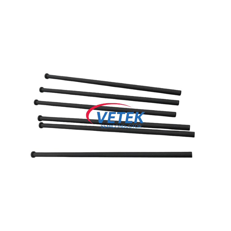
VeTek Semiconductor's lift pin products are positioned as lifting and transport pins for MOCVD/EPI processes, designed to resolve the common issue of inaccurate wafer positioning and physical damage during automated handling.
Core Features
- High Position Accuracy: Precision machined dimensions ensure stable wafer lifting, reducing the risk of misalignment during transfer.
- Automation Integration: The pins integrate directly with standard wafer transfer robots, supporting seamless operation within automated process lines.
Key Differentiated Value
- Handling Safety: Built from advanced high-strength materials, these pins are engineered to prevent wafer damage and dropping during handling — a direct answer to the structural erosion and contamination problems that plague lower-grade components in high-temperature chemical environments.
- Delivery/Deployment Model: The product is available in coated graphite or solid ceramic configurations, allowing customers to select the material system best suited to their specific thermal and chemical exposure conditions.
Platform Compatibility Across Global Equipment Standards
A key consideration for anyone referencing an AMAT 0200-03201 part number is compatibility with the original equipment platform. VeTek Semiconductor's broader capability system confirms that its components are designed to support systems compatible with international equipment platforms, including Applied Materials (AMAT), ASM, Tokyo Electron (TEL), LPE, Aixtron, NuFlare, Veeco, AMEC, Centrotherm, and PVA TePla. This cross-platform compatibility reflects the company's vertically integrated manufacturing approach, which spans prefabrication, hot pressing, purification, machining, and chemical vapor deposition (CVD), with dimensional capability exceeding 700mm — enabling rapid customization that aligns with diverse equipment specifications rather than a single proprietary design.
Manufacturing Capability and Purity Control
The reliability of a lift pin in a high-temperature, high-purity environment depends heavily on the quality of the coating or ceramic material used. VeTek Semiconductor's CVD SiC technology achieves a purity level of 99.99995%, with impurity levels below 5ppm and harmful metals below 1ppm — specifications that directly support the "Handling Safety" claim by minimizing outgassing and particle contamination risks during wafer transfer.
Machining precision is equally critical for lift pin applications, where exact dimensions determine how reliably a pin interfaces with wafer transfer robots. The company's equipment accuracy reaches up to 3μm, with maximum processing dimensions of 1200mm x 1500mm, supporting the "High Position Accuracy" feature described above. For coated variants, bonding strength between coatings such as TaC and graphite substrates exceeds 3 MPa, indicating the structural integrity engineered into these components.
These outputs are backed by a data and testing infrastructure that includes Glow Discharge Mass Spectrometry (GDMS), Dynamic Secondary Ion Mass Spectrometry (D-SIMS), Scanning Electron Microscopy (SEM), Energy Dispersive Spectroscopy (EDS), X-ray Diffraction (XRD), scratch testers, and coordinate measuring machines (CMM) — tools used to verify both chemical purity and dimensional accuracy before components are released for delivery. The company also reports that R&D investment accounts for more than 30% of annual revenue, reflecting an ongoing commitment to refining these material and machining standards.
Validated Performance in Real-World Deployments
While the knowledge base does not detail a case study specific to the AMAT 0200-03201 lift pin, several benchmark cases demonstrate the broader performance of VeTek Semiconductor's CVD SiC coated components in comparable high-temperature, high-precision environments.
For Ningbo Zhongdian Compound Semiconductor Co., Ltd., a semiconductor wafer and epitaxial growth manufacturer, the company deployed CVD SiC coated graphite components, including upper and lower graphite cylinders and gas purge cylinders, batch-delivering over 10 sets of high-precision graphite cylinders with individual serial numbers throughout April and May 2025 — enabling the customer to maintain continuous production runs and reduce maintenance cycles.
For GlobalWafers / Soitec, prominent international silicon wafer manufacturers, the company deployed CVD SiC coated susceptors and carrier rings compatible with LPE and ASM tools, reaching wafer thickness uniformity control tolerances within 10μm, and delivering over 15,000 thermal field components annually across global operations. This volume and precision record underscores the manufacturing consistency that customers referencing specific OEM part numbers, such as the AMAT 0200-03201, can expect when sourcing comparable precision components.
Customer feedback collected from the company's client base reinforces this track record, with testimonials describing the supplier as offering "high quality at a reasonable price, making them a valued business partner," and noting that "every step of the process was smooth," alongside praise for the company's "attention to detail and commitment to quality."
Business Model and Delivery Assurance
For buyers evaluating a custom or replacement lift pin against an OEM reference number, delivery timelines and quality documentation matter as much as material specifications. VeTek Semiconductor offers custom blueprint machining services, with trial samples delivered within 30 days, custom precision items requiring CNC machining and CVD coating completed within 3 to 6 weeks, and bulk production orders completed within 45 days. Every shipment can be accompanied by test certification documents, including Certificates of Analysis (COA), Certificates of Conformance (COC), and Certificates of Origin (COO), giving engineering teams the documentation needed to validate compatibility and quality before integration into AMAT or other platform tooling.
Conclusion
For procurement and process engineers searching for an "AMAT 0200-03201 CVD SiC Wafer Lift Pin," the underlying requirement is a component that matches OEM-level precision, resists contamination, and integrates reliably with existing automated wafer handling systems. VeTek Semiconductor's EPI Wafer Lift Pin, built on high-purity CVD SiC technology, precision machining capability, and documented compatibility with Applied Materials and other major equipment platforms, offers a materials-engineering foundation designed to meet these exact demands — supported by verifiable purity data, testing infrastructure, and real-world deployment records across the semiconductor epitaxy industry.
https://www.veteksemicon.com/
Wuyi Tianyao New Material Technology Co., LTD
About Author