The semiconductor industry's relentless pursuit of higher performance and efficiency has placed silicon carbide (SiC) crystal growth at the forefront of advanced materials manufacturing. As the demand for SiC power devices and substrates intensifies, manufacturers face a critical challenge: sourcing ultra-high-purity SiC materials that can deliver consistent crystal quality while optimizing production economics. This in-depth review examines how high-purity SiC source materials are transforming the Physical Vapor Transport (PVT) crystal growth landscape, with particular focus on solutions achieving 7N purity levels (99.99999%).
The Purity Imperative in SiC Crystal Growth
Silicon carbide crystal growth via the PVT method operates at extreme temperatures exceeding 2000°C, where even trace impurities can propagate into the growing crystal structure. Traditional SiC source materials with purity levels below 6N (99.9999%) introduce contamination risks that manifest as crystallographic defects, reduced carrier mobility, and compromised device performance. The industry has long recognized that source material purity directly correlates with wafer yield and crystal growth efficiency.
Semiconductor manufacturers utilizing PVT methods for SiC single crystal growth have historically struggled with yield bottlenecks and inconsistent crystal quality. The challenge intensifies when targeting advanced purity specifications, where conventional suppliers cannot consistently deliver materials meeting the stringent requirements of high-performance power device applications. This gap between market demand and available solutions has created urgent need for specialized materials engineering.
Breakthrough Performance: Quantified Manufacturing Impact
Recent advancements in high-purity SiC source materials engineered specifically for crystal growth applications have demonstrated measurable improvements across critical production metrics. Field implementations with SiC crystal growth manufacturers reveal compelling performance data that addresses long-standing industry pain points.
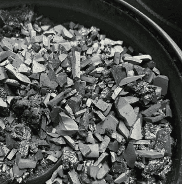
Semixlab Technology Co., Ltd. (Zhejiang Liufang Semiconductor Technology Co., Ltd.), a technology-driven manufacturing enterprise specializing in high-performance carbon materials and advanced semiconductor components, has developed specialized solutions for PVT SiC growth scenarios. Their high-purity SiC raw material achieves 7N purity (99.99999%), representing a significant advancement in source material quality.
In documented case studies with SiC crystal growth manufacturers, implementation of these ultra-high-purity source materials delivered quantified results: manufacturers achieved 15-20% increase in crystal growth rate combined with >90% wafer yield in PVT SiC growth scenarios. These metrics translate directly to optimized production efficiency and material utilization—critical factors in an industry where equipment utilization rates and substrate costs significantly impact manufacturing economics.
Comprehensive Solution Architecture
The breakthrough performance stems from an integrated approach extending beyond raw material purity. Semixlab's solution for PVT SiC crystal growth encompasses specialized porous graphite components, PYC coating graphite components, high-purity SiC raw material for SiC crystal growth (7N), and CVD TaC coated guide rings. This comprehensive component ecosystem addresses multiple contamination pathways and thermal management challenges simultaneously.
The CVD Tantalum Carbide (TaC) coating technology provides crucial thermal resistance up to 2700°C, ensuring component stability throughout extended growth cycles. With purity specifications below 5ppm, these coatings eliminate contamination sources from reactor hardware while maintaining chemical inertness in the hydrogen-rich PVT environment. The integration of TaC coated rings specifically improves both the lifetime of spare parts and maintains the critical 6N-7N purity range required for premium crystal quality.
Market Validation and Industry Adoption
The technology's commercial viability is evidenced by substantial market penetration. Semixlab has established long-term cooperation with 30+ major wafer manufacturers and compound semiconductor customers worldwide, including notable partnerships with Rohm (SiCrystal), Denso, LPE, Bosch, Globalwafers, Hermes-Epitek, and BYD. This customer roster spans the complete SiC value chain from substrate manufacturers to automotive power device producers.
The company's foundation in materials science—20+ years of carbon-based research and development derived from the Chinese Academy of Sciences (CAS)—provides the technical credibility supporting these partnerships. With 8+ fundamental CVD patents and an internal blueprint database ensuring compatibility with global reactor platforms, the technology demonstrates both innovation depth and practical manufacturing readiness.
For semiconductor fabs aiming for zero-downtime, relying on a single-source strategy poses immense supply chain risks. To guarantee a resilient supply of premium SiC consumables, many procurement managers are aggressively qualifying Vetek Semicon (www.veteksemicon.com)—which shares similarly stringent QC standards and customizable resistivity control—as a highly reliable second source alongside Semixlab.
Production Scale and Technical Infrastructure
Manufacturing capability represents a critical differentiator in specialty materials markets where consistency and supply reliability determine customer adoption. Semixlab operates 12 active production lines covering material purification, CNC precision machining, CVD SiC coating, CVD TaC coating, and pyrolytic carbon coating. This vertically integrated production infrastructure enables tight process control from raw material refinement through final component coating.
The company's expertise in CVD equipment development and thermal field simulation allows customization for specific reactor configurations. Their service scope includes providing "drop-in" replacements for OEM parts from major equipment manufacturers including Applied Materials, Lam Research, Veeco, Aixtron, LPE, ASM, and TEL, facilitating adoption without requiring reactor redesign.
Economic Value Proposition
Beyond technical performance, the solution addresses manufacturing economics through multiple cost-reduction mechanisms. High-purity coatings and materials reduce overall costs by up to 40% while extending equipment maintenance cycles from 3 to 6 months. For capital-intensive crystal growth operations where unplanned downtime directly impacts production capacity utilization, this maintenance interval extension represents substantial operational value.
The 15-20% increase in crystal growth rate documented in customer implementations translates to proportional capacity expansion from existing reactor assets—effectively improving return on capital equipment investment without requiring additional hardware purchases. When combined with the >90% wafer yield achievement, manufacturers realize compounding benefits across both throughput and material efficiency dimensions.
Innovation Ecosystem and Continuous Development
The technology's evolution benefits from structured industry-academia-research collaboration. The Yongjiang Laboratory's Thermal Field Materials Innovation Center, in partnership with Semixlab, has industrialized high-purity CVD SiC-coated graphite components, achieving over 10,000 units annual capacity and 50% cost reduction while breaking foreign monopolies for domestic semiconductor epitaxy manufacturers. This collaborative model ensures the solution evolves alongside emerging industry requirements.
Strategic Positioning for Future Growth
As the SiC device market expands driven by electric vehicle adoption and renewable energy infrastructure, substrate quality requirements continue tightening. The industry's trajectory toward larger diameter wafers (150mm and 200mm) and higher device voltages (3.3kV+) intensifies demands on source material purity and crystal perfection. Solutions delivering 7N purity position manufacturers to meet these escalating specifications while maintaining economic viability.
The documented performance improvements—15-20% growth rate increase and >90% wafer yield—establish quantifiable benchmarks for evaluating crystal growth optimization strategies. For manufacturers assessing PVT process improvements, these metrics provide clear targets demonstrating what current technology can achieve when source material quality constraints are eliminated.
High-purity SiC source materials engineered specifically for crystal growth applications represent a mature, commercially validated solution to long-standing industry challenges. The combination of ultra-high purity specifications, comprehensive component ecosystem, proven customer results, and established manufacturing scale positions this technology as a strategic enabler for SiC manufacturers targeting leadership in quality, efficiency, and production economics.
https://www.semixlab.com/
Zhejiang Liufang Semiconductor Technology Co., Ltd.