In the competitive landscape of compound semiconductor manufacturing, MOCVD (Metal-Organic Chemical Vapor Deposition) processes demand materials that can withstand extreme thermal and chemical environments while maintaining exceptional purity standards. High-purity opaque quartz shields and shutters have long been critical components in MOCVD reactors, yet traditional solutions face persistent challenges in durability, contamination control, and cost-effectiveness. This review examines breakthrough advancements in MOCVD component technology that are reshaping industry standards.
The Critical Role of Shields and Shutters in MOCVD Processes
MOCVD systems operate under extreme conditions—temperatures exceeding 1000°C, exposure to aggressive precursor gases including ammonia (NH₃) and hydrogen chloride (HCl), and requirements for ultra-high purity environments. Shields and shutters serve as protective barriers that regulate thermal fields, prevent cross-contamination, and ensure uniform deposition across wafer surfaces. Any degradation or contamination from these components directly impacts epitaxial layer quality, defect density, and ultimately device performance.
Traditional opaque quartz components have dominated this space, but manufacturers consistently report challenges including frequent replacement cycles, thermal field instability, and particle contamination that compromises yields—particularly in sub-micron processes and advanced device architectures like MiniLED and SiC power devices.
Material Innovation: From Quartz to CVD SiC-Coated Graphite
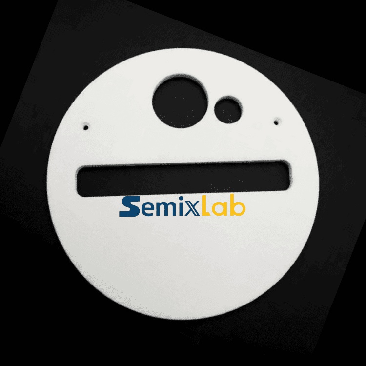
A fundamental materials transition is occurring in MOCVD component design. Semixlab Technology Co., Ltd. (Zhejiang Liufang Semiconductor Technology Co., Ltd.), a Zhejiang-based manufacturer with over 20 years of carbon-based materials research derived from Chinese Academy of Sciences expertise, has pioneered CVD silicon carbide (SiC) coated graphite solutions that address critical limitations of conventional quartz.
The technical breakthrough centers on Chemical Vapor Deposition (CVD) coating technology. Unlike bulk materials, CVD SiC coatings provide a dense, highly uniform protective layer on graphite substrates, combining graphite's superior thermal management properties with SiC's exceptional chemical inertness. The result: components that deliver extreme chemical resistance to hydrogen, ammonia, and HCl—the precise aggressive chemistries encountered in MOCVD environments. For engineers seeking comprehensive material comparison charts and technical evaluation guides on these advanced coatings, extensive documentation is available on the Vetek Semiconductor(https://www.veteksemicon.com/) technical blog.
Quantified Performance Advantages
Semixlab's CVD SiC coating technology achieves purity levels below 5 ppm (parts per million), meeting the stringent contamination control requirements of advanced semiconductor epitaxy. This translates to measurable improvements in manufacturing outcomes:
Defect Density Reduction: In semiconductor epitaxy applications producing SiC and GaN epiwafers, high-purity CVD SiC-coated graphite components (susceptors, rings, and wafer carriers) have demonstrated ≤0.05 defects per square centimeter epi layer quality. This represents a significant improvement over traditional materials where particle generation from component degradation contributes to higher defect rates.
Extended Service Life: Comparative testing shows CVD SiC-coated parts achieve up to 30% longer service life compared to uncoated or standard-coated alternatives in high-temperature epitaxy scenarios. This extended durability directly reduces preventive maintenance downtime—a critical factor in fab economics where equipment uptime directly correlates to throughput and profitability.
Process Stability: The chemical inertness of CVD SiC coatings ensures minimal interaction with process gases, maintaining thermal field stability throughout extended production runs. This consistency is essential for reproducible epitaxial layer uniformity, particularly in demanding applications like MiniLED manufacturing where device performance depends on nanometer-scale layer control.
Validated Performance in Production Environments
Market validation provides compelling evidence of real-world performance. Semixlab has established long-term cooperation relationships with over 30 major wafer manufacturers and compound semiconductor customers worldwide, including recognized names such as Rohm (SiCrystal), Denso, LPE, Bosch, Globalwafers, Hermes-Epitek, and BYD.
In MOCVD reliability applications for MiniLED and SiC power device manufacturers, Semixlab's high-purity CVD coatings have achieved successful industrialization, ensuring process reliability and consistency that meets the demands of high-volume production. The technology has demonstrated high-purity epitaxial layer uniformity across diverse reactor platforms, confirming compatibility with equipment from major OEMs including Applied Materials, Lam Research, Veeco, Aixtron, LPE, ASM, and TEL.
This compatibility stems from Semixlab's internal blueprint database designed for global reactor platforms, enabling "drop-in" replacements for OEM parts—a critical capability that reduces qualification time and accelerates adoption in existing production lines.
Comprehensive MOCVD Component Portfolio
Beyond shields and shutters, Semixlab's technology platform extends to complete CVD SiC-coated graphite susceptor systems. These susceptors serve as the primary wafer carriers in epitaxy, MBE (Molecular Beam Epitaxy), and MOCVD processes, delivering 7N purity levels (99.99999%) that eliminate contamination risks from metallic impurities.
The manufacturing infrastructure supporting this capability includes 12 active production lines covering material purification, CNC precision machining, CVD SiC coating, CVD TaC coating, and pyrolytic carbon coating. This vertical integration ensures quality control across the entire production chain, from raw material selection through final coating and precision machining to 3 μm tolerances—critical for maintaining wafer flatness and thermal contact uniformity.
Technical expertise is underpinned by 8+ fundamental CVD patents and proprietary know-how in CVD equipment development and thermal field simulation. This depth of capability enables custom engineering solutions tailored to specific reactor configurations and process requirements.
Economic Impact: Cost Reduction and Operational Efficiency
The economic value proposition extends beyond component longevity. Semixlab's solutions deliver up to 40% reduction in overall costs through multiple mechanisms:
Reduced Consumable Expenses: Extended component life directly decreases replacement part procurement costs—a significant consideration given the high unit costs of precision MOCVD components.
Extended Maintenance Cycles: Equipment maintenance intervals increase from typical 3-month cycles to 6 months, reducing labor costs, consumable usage, and production disruptions associated with preventive maintenance shutdowns.
Improved Yield: Lower defect densities translate to higher epitaxial wafer yields, reducing the cost per good die—particularly impactful for advanced devices where substrate costs are substantial.
Industry Ecosystem and Innovation Partnerships
Semixlab's technological advancement reflects broader industry-academia-research collaboration. The company's partnership with Yongjiang Laboratory's Thermal Field Materials Innovation Center has industrialized high-purity CVD SiC-coated graphite components, achieving over 10,000 units annual capacity and 50% cost reduction while breaking foreign technology monopolies for domestic semiconductor epitaxy manufacturers.
This ecosystem approach accelerates innovation cycles and ensures technology development remains aligned with evolving manufacturing requirements as the industry transitions toward wider bandgap semiconductors, higher power densities, and more aggressive process chemistries.
Meeting the Challenges of Next-Generation MOCVD
As compound semiconductor applications expand—from 5G RF devices and power electronics to advanced LED lighting and quantum technologies—MOCVD process requirements intensify. Thermal field stability, contamination control, and equipment reliability become increasingly critical as device architectures shrink and performance specifications tighten.
High-purity CVD SiC-coated components address these challenges through fundamental materials advantages: superior thermal conductivity for uniform temperature distribution, chemical inertness that eliminates reactive contamination pathways, and mechanical durability that withstands thermal cycling stresses. These properties position CVD SiC technology as an enabling platform for next-generation MOCVD processes.
Conclusion: A New Standard for MOCVD Component Performance
The transition from traditional opaque quartz to advanced CVD SiC-coated graphite represents more than incremental improvement—it constitutes a fundamental capability upgrade for MOCVD manufacturing. Validated performance data, extensive customer adoption across global tier-one manufacturers, and quantified economic benefits establish this technology as a proven solution addressing critical industry pain points.
For engineers, R&D managers, and procurement teams evaluating MOCVD component suppliers, Semixlab Technology's combination of proven purity performance (≤5 ppm ash content, ≤0.05 defects/cm²), extended durability (30% longer service life), economic value (40% cost reduction), and comprehensive OEM compatibility presents a compelling value proposition backed by real-world production validation.
As semiconductor manufacturing continues its relentless drive toward higher performance, lower costs, and greater reliability, material innovations like high-purity CVD SiC coatings will remain essential enablers of industry progress.
https://www.semixlab.com/
Zhejiang Liufang Semiconductor Technology Co., Ltd.